Shuriken Video (powered by gcvideo)
Overview
Use this design at your own risk, I take no responsibility for any damaged caused if anything goes wrong.
I wanted to be able to connect my gamecubes video output to the HDMI port of my TV / PC monitor, I know that the first versions of the gamecubes had a digital video port as well as an analogue port. I wondered if some how it could be connected to a HDMI converter. I looked around and found this guys work
https://github.com/ikorb/gcvideo
This guy is good I mean really good I download his work and tried to find fault with it, I really tried to find some errors but all I found was my misunderstanding or lack of knowledge I simple cant find fault with his work its great! Basically he uses a small FPGA to read the gc digital port and converts the signals into standard DVI protocol of reception by a DVI / HDMI TV / PC monitor, perfect for what I need :-)
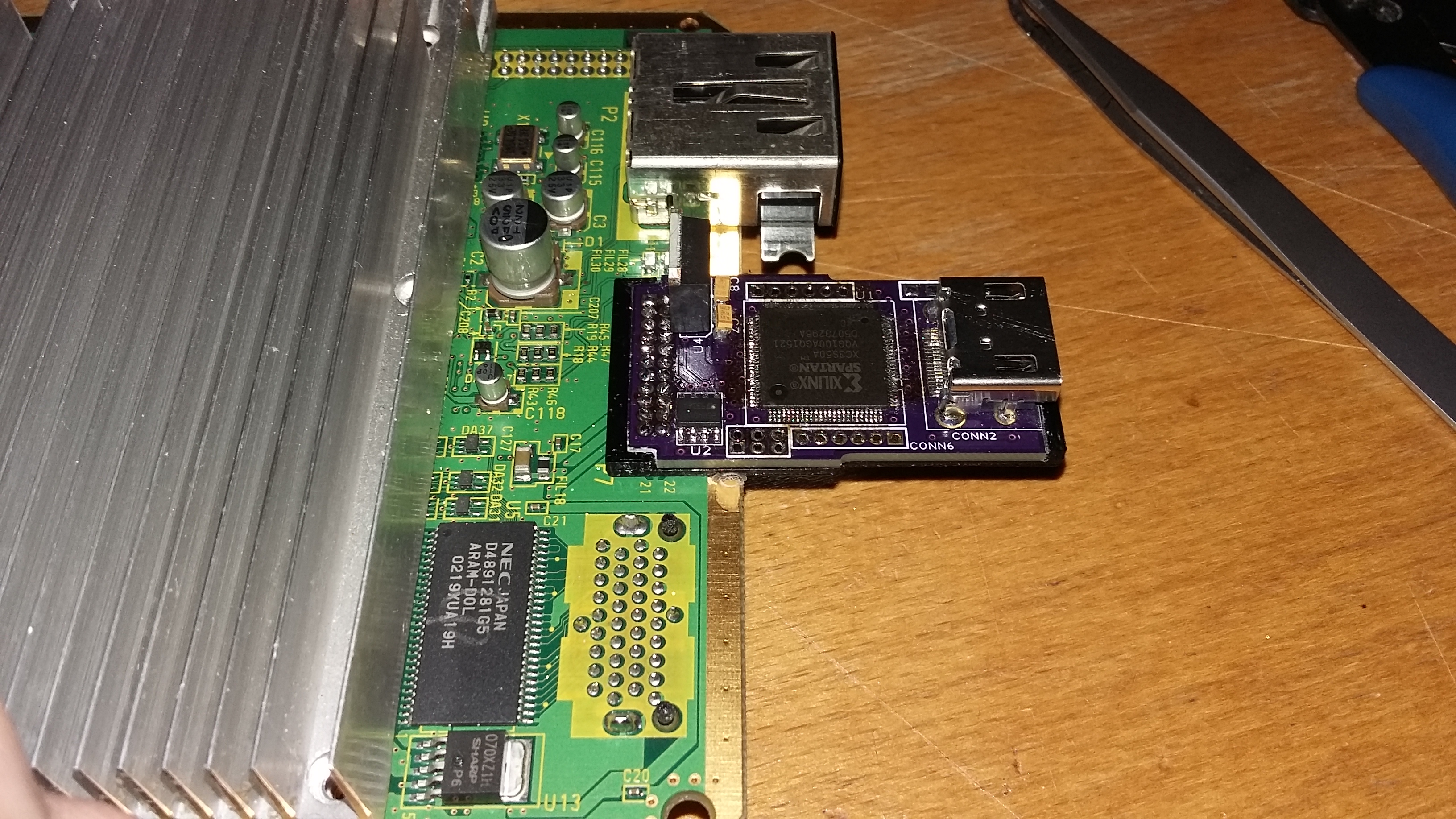
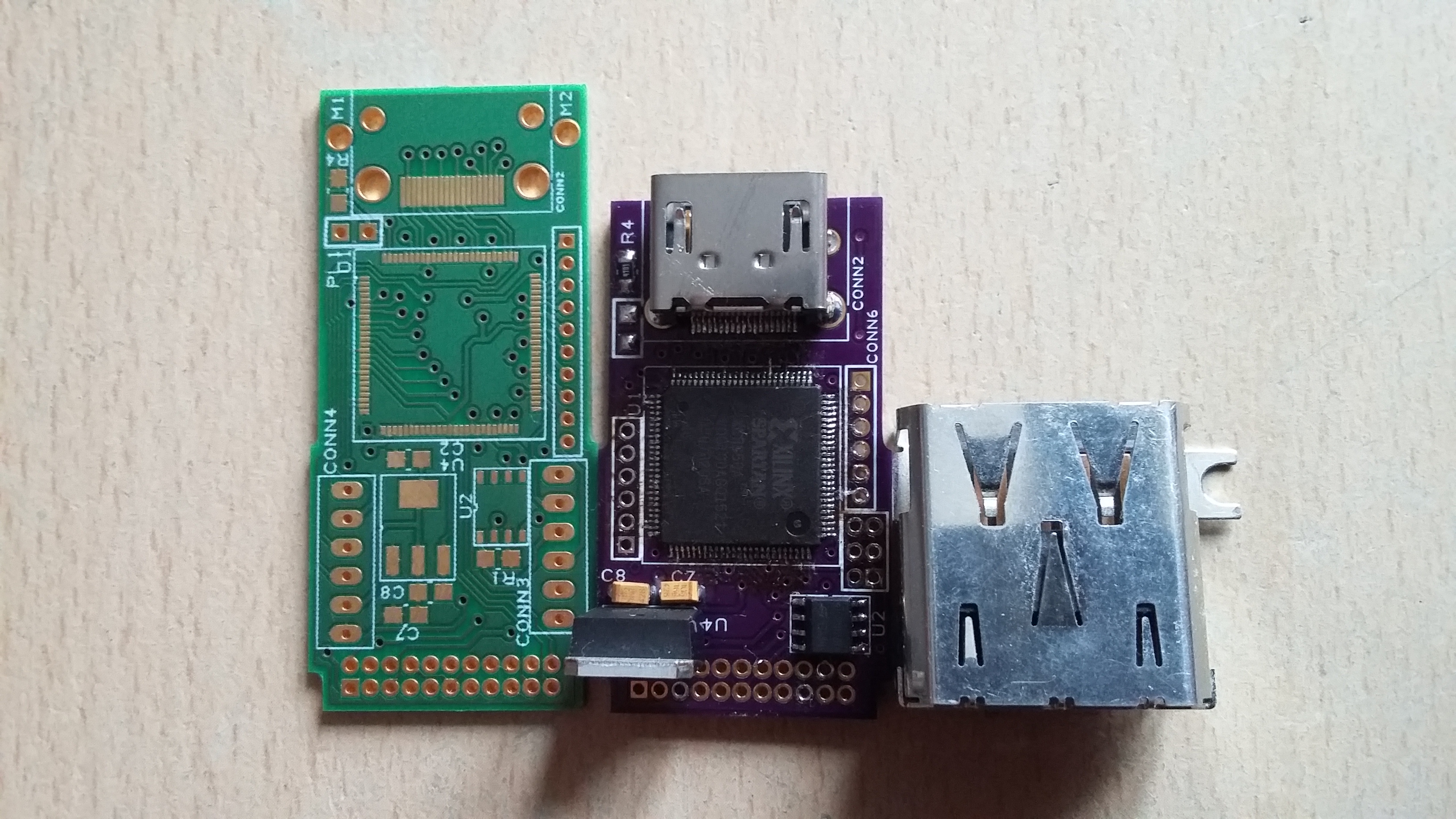
Shuriken Video PCB overview
gcvideo dvi runs on a Pluto IIx HDMI board, which uses a xc3S200a xilinx FPGA, to reduce cost and make an open source project I created a Shuirken Video PCB which uses a xc3S50a xilinx FPGA and is targeted at the gamecube only (its not a general development board).
Schematic V1 & V2
Note: C7 should be 4.7uF and C8 should be 1uF both tantalum type caps to reduce noise.
This schematic (pdf) basically shows the FPGA wiring between the gamecubes digital port and HDMI connector, the real schematic file is part of the artwork package below.
Schematics V3
Note: C7 should be 10uF and C8 should be 100nF so that the 3.3V supply rail raises before the 1.2V rail (next version going to have a proper reset IC).
This schematic (pdf) is the for the slightly smaller version 3 of the PCB board.
PCB software
Because this project is open source I decided to use RS design sparks http://www.rs-online.com/designspark/electronics/ software for creating the PCB.
PCB artwork V1 - prototype
here is the artwork for the Shuriken Video board V1 this includes the schematic and PCB files.
PCB artwork V2
I made the board slightly smaller so that it would fit into the gamecube with minor modifications to the gamecube's case here are the updated files.
PCB artwork V3
Made the board slightly smaller again here are the updated files the board plots are under plots\video_v3_3_plots.zip (osh format).
Part numbers / BOM for V1 & V2 boards
All part numbers are from farnell
225-3716 Serial flash 4Mbit 8SOIC
185-1995 1.2v reg SOT223 (for boards that don't use a SPDIF connector due to the current limit of 1A on these devices)
182-5292 5v reg SOT223
151-6661 HDMI connector
167-1088 XC3S50A-4VQG100C
resistors / caps are all 0805
Part numbers / BOM for V3 boards
Here's the BOM for V3 it includes farnell part numbers total cost £6.12 that don't include the price of the FPGA.
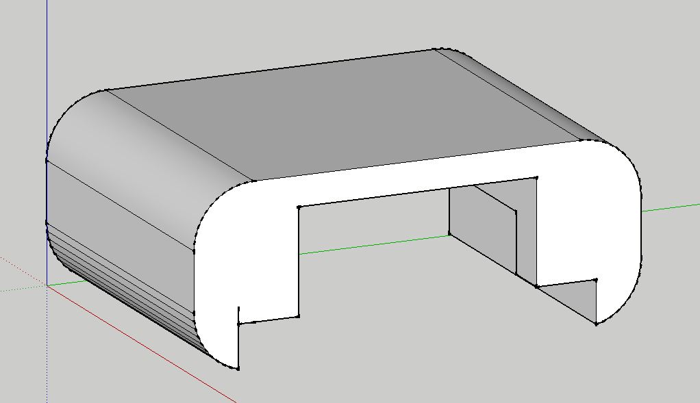
3D case
Updated 5/7/2015
Here is the bottom half of the 3D case for the prototype board (V1) its a quick hack up done in google sketchup. This next one is much better its bottom half of the 3D case for version 2 of the PCB again done in google sketchup here are the design files.
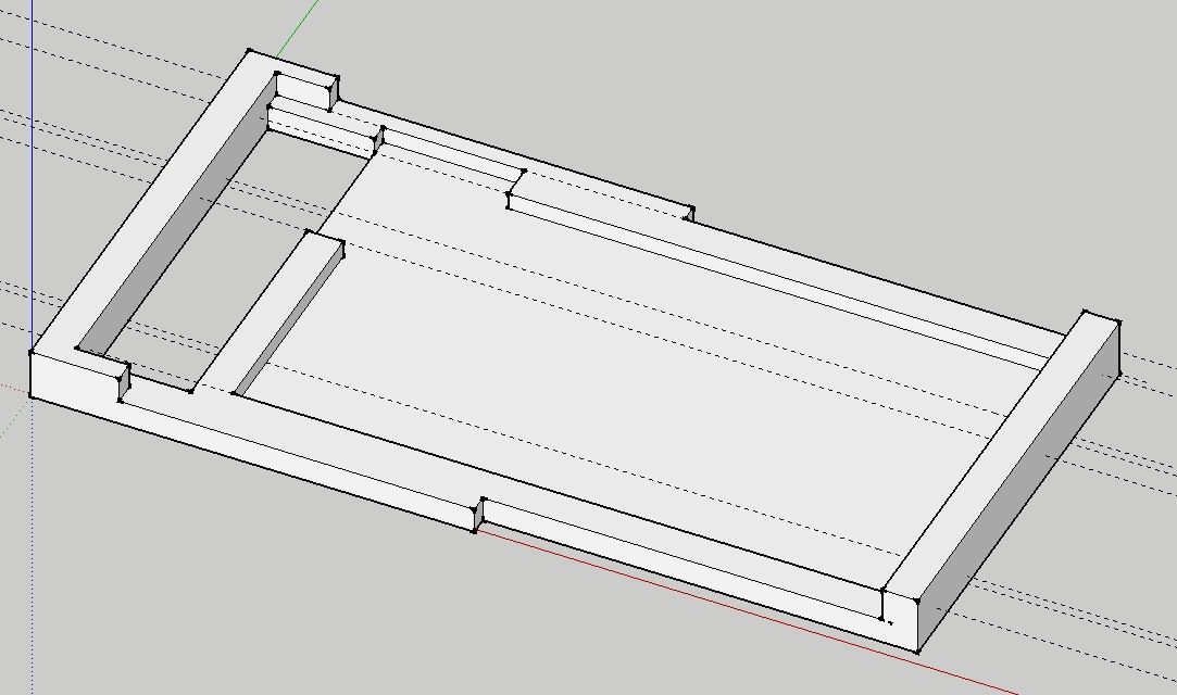
Updated 17/2/2016
Here is the top case for the shuriken v3 board
Here is the bottom case for the shuriken v3 board
gcvideo for shuriken board
I have code ported the gcvideo vhdl files to work with my board (which uses the xc3S50a and different pinouts) here are the modified files.
Updated 2/7/2015
Added SPDIF support (audio) from main source branch here is the re-build, SPDIF is outputted on pin 8 of the spare connector.
Updated 25/8/2015
Updated code to pull in changes from main branch (gcvideo-dvi version 2.0), here is the re-build. From gcvideo-dvi version 2.0 audio over HDMI interface is now supported however to get the updated base line to fit inside the xc3S50a I had to remove support for the SPDIF output.
Updated 1/9/2015
played with the compiler options and managed to fit the SPDIF encoder logic back into the build (thanks dude) so here is an update with audio over HDMI and SPDIF output !
Programming the shuriken board
Xilinx ISE IDE software creates a *.bit file which is used to program via JTAG the FPGA, however this board is designed to load it configuration information from a spi serial flash device ( M25P40). So it needs a slightly different file for programming. To create this I used xilinx's command prompt promgen program and run it using the following parameters
promgen -spi -p bin -o spi_flash.bin -s 512 -u 0 toplevel_p2xh.bit
This creates a binary file spi_flash.bin which I used to program the board (see xilinx app951 page 13 for more details). To program the board you simple connect JP1 this pulls prog_b low and forces the FPGA into standby mode allowing a flash programmer direct access to the spi flash chip. Then you connect your programmer to the serial flash port (conn3 on the PCB) and flash down the *.bin file. To flash down the binary file I used my own program here, (note tested using a XP machine using this i/o driver I think (placed in c:\windows\system32\drivers) but this uses a parallel port to bit bang the spi flash commands / data to the chip which most computers do not have anymore.
Update 17/2/2016
My old PC with a parallel port finally died so I had to find another way to program the serial flash device. If you have one of these Lcsoft CY7C68013A Mini Board (cypress FX2LP)
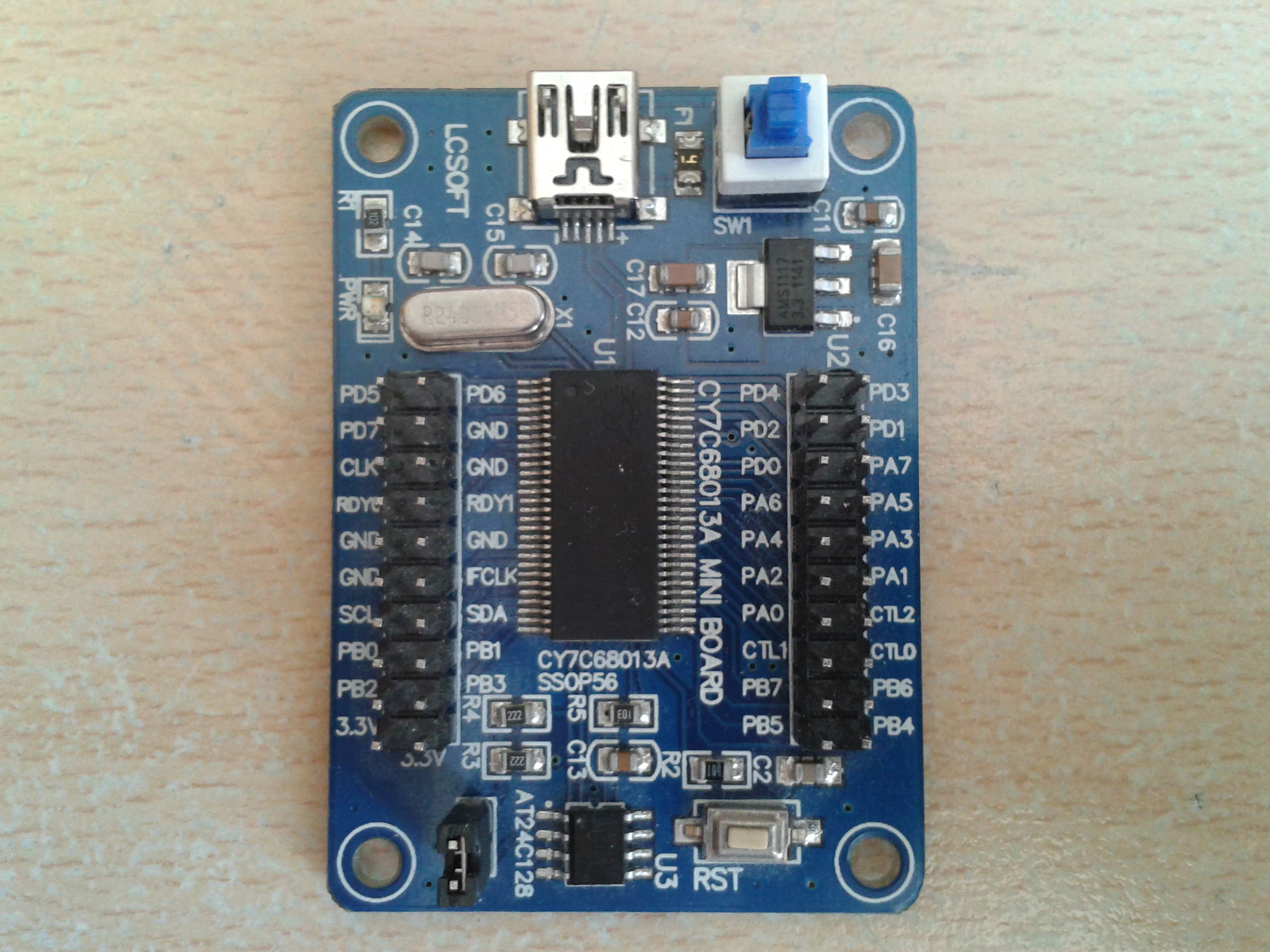
which I found on ebay for £10. Application note AN58764 from cypress turns the board into a USB to serial port, I modified this application note (modified code here) to flash the receive data from the PC into the M25P40. Download the modified application note into the board (if you want the board to remember that's its a serial port between power cycles follow app note AN45197) and then connect the board to the M25P40 as follows
PCB M25P40 CY7C68013A
4 CLK
PA0
1
MOSI
PA1
2
MISO
PA2
3
SS
PA3
5
GND
GND
Finally connect the CY7C68013A Mini Board to the PC via a USB cable, the board should show up as an extra comm port then use this PC program I created like this
new_fpga_flash.exe COM1 program.bin
Where COM1 is the name of the new com port on your PC and program.bin is the program you want to flash into the M25P40 device.
Or If you have a JTAG programmer you can follow the instructions on page 13 of xilinx app951 which basically creates a *.mcs file instead of a bin file and uses iMPACT to flash this file into the spi serial flash chip.
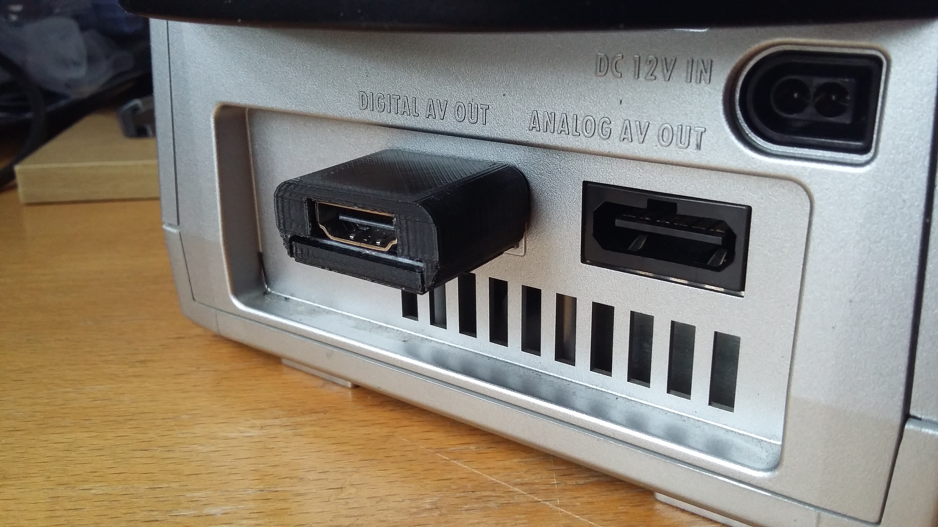
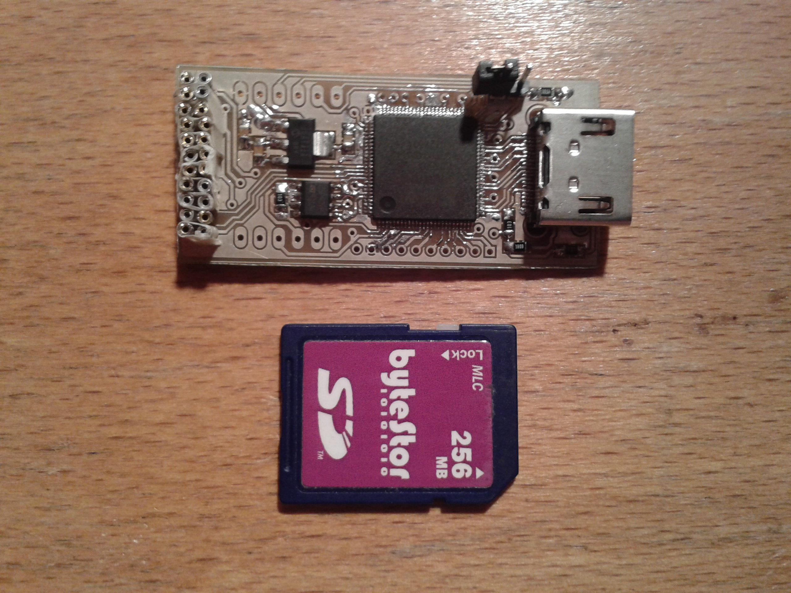
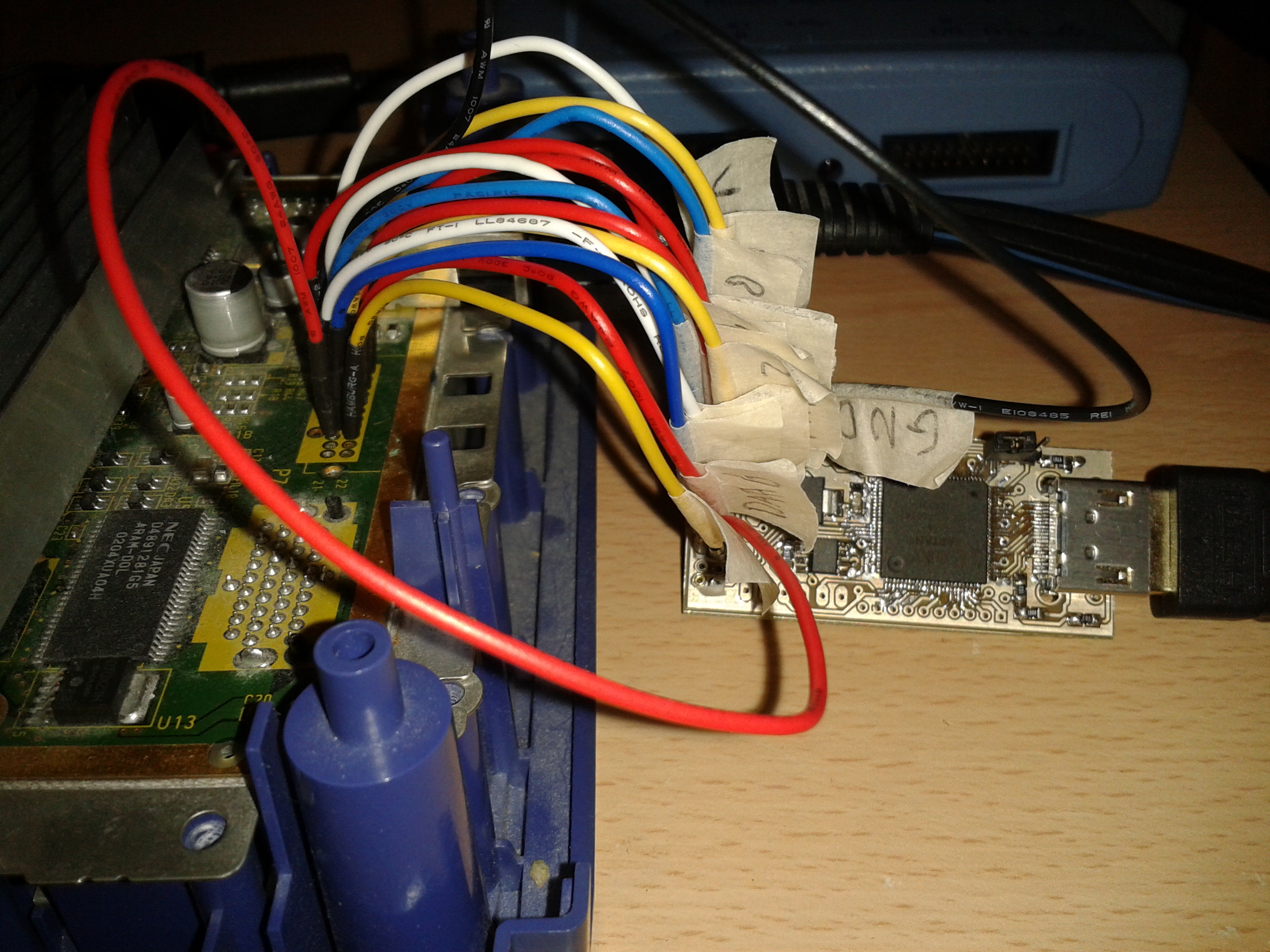
Shuriken Video pictures
Finally some project pictures v1 & v3