GC DSP
References:
gc_dsp.pdf (by duddie)
DSP56100.pdf
DSP56156UM.pdf
U.S. Pat. 7,369,665 (Method and apparatus for mixing sound signals)
DSPSPY (source code)
DSPTOOL (source code)
dsp_info.txt (by org)
Tools used:
IDA Pro with python GCDSP plugin.
Overview:
I want to learn a bit more about the gamecubes DSP chip so I am going to play around with it and post anything interesting I find.
26/02/2016
DSP mailbox's
Been reading through the user manual for the DSP56156 and although the op-codes don't match the overall architecture of the device seems to match the dsp chip inside the gamecube quite well. For example org wrote this in dsp_info.txt
'Mailbox Registers
-------------------------
0x0C005000 DSP Output Mailbox Register High
Part (CPU->DSP)
0x0C005002 DSP Output Mailbox Register Low Part (CPU->DSP)
0x0C005004 DSP Input Mailbox Register High Part (DSP->CPU)
0x0C005006 DSP Input Mailbox Register Low Part (DSP->CPU)
Although patent is said they are 32-bit wide, Nintendo DSP library accessing
them by 16-bit halfs. I dont know reason of that.'
If you look under section 5 of DSP56156 (host interface) you see that the device has a memory mapped i/o port in the user manual this ports registers HTX and HRX (figure 5.1) are only 16bits wide however if you had two sets of HTX and HRX to make the width 32bits you would have to access them the way org describes. Say you wanted to send something to this new imaginary DSP56156 device you would first write16 bits to 0x0C005000 which would fill up TXH register (if it was memory mapped to 0x0C005000) then you would write to the lower register 0x0C005002 which would fill up TXL. Yes you can just write all 32bits at once as they are memory mapped however there is a problem with doing this. The manual states
'These registers may be written in any order
to transfer 8 or 16-bit data. However, writing the
Transmit Low register TXL clears the TXDE bit. Because writing the TXL register
clears
the TXDE status bit, TXL is normally the last register written during a 16-bit
data transfer.'
so basically its saying Transmit Data Register Empty (TXDE) bit will be cleared on a write to the lower memory mapped address. You dont want this bit to go low before the whole 32bits of data has been written onto the dsp chip, so its better to write the upper 16bits into TXH and then the lower 16 bits into TXL to guaranty that TXDE only goes low when valid information is present in the dsp chip. What's so special about TXDE anyway? Well this leads me onto the next part of dsp_info.txt org wrote
'Another questionable thing is high-order bit
of mailbox registers. DSP
library is checking this bit all the time, after writing/reading mailboxes :
// mail delivered to DSP ?
u32 DSPCheckMailToDSP(void)
{
return ( *(u16 *)0xCC005000 & 0x8000 );
}
After you write data into memory mapped host interface registers TXH and TXL goes low because those registers are not empty anymore this will then trigger the movement of data from TXH & TXL into the HRX's registers (providing they are empty) at this point TXDE goes high again (section 5.5 of the user manual). I believe TXDE is mapped to bit 16 of mailbox 0xCC005000, so basically after writing data into the dsp chip bit 16 of 0xCC005000 will be low until the data has been moved to HRX at which point bit 16 of 0xCC005000 goes high and its safe to transfer the next 32bits of information.
Memory Map
Its also interesting that the memory map of the gamecubes dsp chip and the dsp56156 seems to match quite closely as well. Looking at hermes.s within the DSPTool source (under Testdata) and cross referencing it dps_info.txt we have the following defined memory areas.
DSCR: equ
0xffc9 ; DSP DMA Control Reg
DSBL: equ 0xffcb
; DSP DMA Block Length
DSPA: equ 0xffcd
; DSP DMA DMEM Address
DSMAH: equ 0xffce
; DSP DMA Mem Address H
DSMAL: equ 0xffcf
; DSP DMA Mem Address L
Accelerator ARAM Starting Address High:
0xFFD4
Accelerator ARAM Starting Address Low: 0xFFD5
Accelerator ARAM Ending Address High: 0xFFD6
Accelerator ARAM Ending Address Low: 0xFFD7
Accelerator ARAM Current Address High: 0xFFD8
Accelerator ARAM Current Address Low: 0xFFD9
ARAM DMA request Mask: 0xFFEF
DIRQ: equ
0xfffb ; DSP Irq Request
DMBH: equ 0xfffc
; DSP Mailbox H
DMBL: equ 0xfffd
; DSP Mailbox L
CMBH: equ 0xfffe
; CPU Mailbox H
CMBL: equ 0xffff
; CPU Mailbox L
then if we also look at dump_roms.ds from DSPSpy/util/ we have these defined memory areas
iram 0x0000 - Exception vectors
IROM_BASE: equ 0x8000
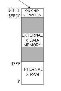
If you then look at user manual for dsp56156 section 3 figure 3-2 you see the following layout which matches the above defined areas
ok the interrupt vector size don't match as the gamecubes dsp chip only as 8 vectors but the general layout looks correct.
14/03/2016
DSP boot up
The boot sequence looks different from dsp56156 it looks like the gamecubes cpu brings the dsp chip out of reset it starts executing code from irom at location 0x8000. Both the wii and gamecube dsp boot roms look the same to me they both start by sending 0x8071feed to the hosts mailbox's and then enter into a command processing loop. The pseudo code below shows the basic loop structure
The gamecubes cpu uses this loop to transfer any required ram variables from main memory into the dsp's dram area. After this it then uses the loop to transfers a small program (ucode task) into the dsp's iram memory area and requests that the dsp chips jumps to this program.